
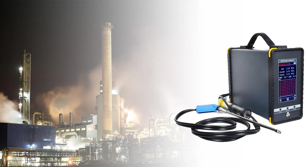
Optical Gas Analysis Solutions in Semiconductor Manufacturing: Ultra-High Precision Monitoring
Semiconductor manufacturing demands extreme precision at every stage of the process. Even trace levels of gas contamination can affect wafer quality, reduce yield, and increase production costs. Monitoring gases such as NH₃, HF, HCl, O₂, and moisture at ultra-low concentrations is essential for maintaining process stability.
optical gas analysis solutions have become critical in semiconductor environments because they provide high-precision, real-time measurement with minimal drift and fast response times, ensuring consistent control in ultra-clean and high-sensitivity processes.
Why Semiconductor Gas Monitoring Is Uniquely Demanding
Semiconductor fabrication environments require a level of accuracy and reliability that far exceeds most industrial applications.
| Challenge | Impact on Production |
|---|---|
| Trace gas contamination | Reduced wafer yield |
| Ultra-low detection levels | Requires ppb-level sensitivity |
| Cleanroom environments | Strict contamination control |
| Rapid process cycles | Need for real-time response |
| High-value production | Zero tolerance for measurement errors |
Even minor deviations in gas concentration can lead to significant financial losses.
optical gas analysis solutions provide the precision and stability required to maintain consistent semiconductor production quality.
Key Gas Monitoring Points in Semiconductor Processes
Gas analysis is integrated across multiple fabrication stages.
| Process Area | Key Gases | Purpose |
|---|---|---|
| CVD / Deposition | NH₃, SiH₄, H₂ | Process control |
| Etching | HF, HCl, Cl₂ | Precision etching control |
| Cleanroom air monitoring | O₂, moisture | Contamination prevention |
| Exhaust systems | VOCs, acids | Environmental safety |
Accurate monitoring ensures stable process conditions and prevents contamination.
optical gas analysis solutions enable real-time tracking of gas composition throughout the semiconductor manufacturing process.
Technology Selection for Ultra-High Precision
Different optical technologies are used depending on the required sensitivity and gas type.
| Technology | Best for Applications | Key Advantage |
|---|---|---|
| TDLAS | Trace gas detection | ppb-level accuracy, low drift |
| UV | Reactive gases (HF, Cl₂) | High sensitivity |
| NDIR | Background gases (CO₂) | Stable and cost-effective |
Selecting the correct technology ensures reliable detection at extremely low concentration levels.
optical gas analysis solutions often integrate TDLAS and UV technologies to achieve both high sensitivity and stability.
Measurement Accuracy and Response Time
Precision and speed are critical in semiconductor processes.
| Parameter | Conventional System | Optical Gas Analysis Solutions |
|---|---|---|
| Detection Limit | ppm | ppb |
| Response Time | Seconds | Milliseconds |
| Measurement Drift | Moderate | Minimal |
| Data Stability | Variable | High |
Higher accuracy and faster response enable better process control and improved yield.
optical gas analysis solutions provide real-time data that allows immediate adjustments in high-speed production environments.
Cleanroom Compatibility and System Design
Gas analyzers must operate without introducing contamination into cleanroom environments.
| Requirement | Solution Feature |
|---|---|
| Particle-free operation | Sealed optical design |
| Low outgassing materials | Cleanroom-compatible components |
| Compact design | Easy integration into equipment |
| Remote monitoring | Reduced physical intervention |
System design must align with strict cleanroom standards to ensure process integrity.
optical gas analysis solutions are engineered to meet cleanroom requirements while maintaining high performance.
Impact on Yield and Production Efficiency
Accurate gas monitoring directly affects semiconductor yield and operational efficiency.
| Parameter | Without Optimization | With Optical Gas Analysis |
|---|---|---|
| Yield rate | 85–90% | 92–98% |
| Defect rate | Higher | Reduced by 20–40% |
| Process stability | Variable | Highly stable |
| Production downtime | Occasional | Minimal |
Improved gas control leads to higher yield and lower production costs.
optical gas analysis solutions help maintain consistent process conditions, reducing defects and improving overall efficiency.
Integration with Semiconductor Equipment
Modern semiconductor manufacturing relies on highly integrated systems.
| Integration Feature | Operational Benefit |
|---|---|
| Equipment-level integration | Direct control within process tools |
| Real-time data output | Immediate process adjustments |
| Remote diagnostics | Faster troubleshooting |
| Automation compatibility | Supports smart manufacturing |
Seamless integration enhances both process control and system efficiency.
optical gas analysis solutions support advanced integration with semiconductor manufacturing equipment and automation systems.
Customization and OEM Capabilities
Semiconductor projects often require highly specialized solutions.
| Customization Area | Benefit |
|---|---|
| Ultra-high sensitivity | Detection of trace gases |
| System miniaturization | Integration into compact equipment |
| Material selection | Cleanroom-compatible materials |
| OEM / ODM support | Custom branding and system integration |
Customized solutions ensure compatibility with highly specialized semiconductor processes.
optical gas analysis solutions with strong OEM/ODM capabilities enable system integrators to meet demanding industry requirements.
Production Capacity, Lead Time, and Quality Control
High-end industries require strict manufacturing standards and reliable delivery.
| Factor | Requirement |
|---|---|
| Production Capacity | Support for precision manufacturing |
| Lead Time | Typically 3–6 weeks |
| Quality Control | Multi-stage calibration and testing |
| Certification | Compliance with global standards |
Reliable production ensures consistent performance across all delivered systems.
optical gas analysis solutions from experienced manufacturers provide the quality and reliability required for semiconductor applications.
Conclusion
Semiconductor manufacturing requires ultra-high precision gas monitoring to maintain yield, quality, and process stability. Selecting the right technology and system design is critical for achieving these goals.
optical gas analysis solutions provide the accuracy, speed, and reliability needed for modern semiconductor environments, enabling real-time control and long-term operational efficiency.
Instrava is a partner focused on providing equipment, solutions, and services for industrial measurement and control instruments used in safety-critical and process control applications. We deliver customized optical gas analysis solutions for semiconductor industries worldwide, supported by advanced technology, strict quality control, flexible OEM/ODM capabilities, and reliable production capacity—helping customers achieve precision-driven manufacturing excellence.